By Ben Nitkin on
For my trinket, I wanted to make the front side unmasked copper, since it's shiney and reflective and looks cool. KiCad supports converting graphics to component files, but only for the silkscreen (user text) and soldermask (the green stuff) layers. But, with the new plaintext components, it's trivial to get graphic copper. Here's how.
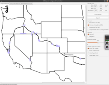
 Start by opening Bitmap2Component. From the main KiCad window, it's the icon to the side here. That'll open the program shown below. You can follow the usual way of creating a component: click on Load Bitmap, adjust the threshold value to select which parts are in the component file, and so on. The Black&White tab shows the final outline. For copper, try to use a resolution above 300dpi (600 or 1200 is best); modern processes can create really, really small features, and you want to take advantage of that. When you're done, save it as a Pcbnew file (.kicad_mod). It doesn't much matter which layer you use, but I'll pretend you're using the Front Silk Screen layer.
 I used the GIMP extensively to modify the source image. Some of the cuts in the copper allow for LED footprints, others divide the contigous USA into a few separate electrical nets. Don't expect KiCad DRC (design rule checking) to work on a bitmap outline, so be very careful with any parts that are also nets.
 Here's the magic sauce: the .kicad_mod file is plain text. Open it up in a text editor, and do a find and replace. In my case, I replaced all instances of F.SilkS with F.Cu to move the component to the top copper layer. (B.Cu would be the back, or you could manually flip it in KiCad with the F hotkey.)
 Save that file and bring it into Pcbnew, either by associating it with a footprint in your schematic layout, or by importing it directly. (You'll need to move it into a folder named "somethingorother.pretty", then add the somethingorother library to Pcbnew.) I made up an inverted version of the copper symbol for a soldermask symbol. That way, the copper was left uncovered, which makes for a really cool looking PCB. If you're interested, look into my other articles on the USA trinket.
That's it, really. Aren't plaintext files great?